

2D Holographic Array Standards
Precision, holographic pattern providing accurate calibration in the horizontal plane for very high resolution, nanometer-scale measurements with 144nm and 300nm pitch.
 |
 |
|||||
| Model 2D/144nm Pitch | Model 2D/144nm Pitch | |||||
|
144nm Very High Resolution 2D Calibration Standard for AFM, STM, Auger, FIB, and SEM |
||||||
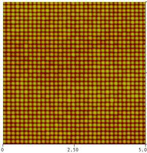
| Period: | 144nm pitch, two-dimensional array. Accurate to ±1nm. Refer to calibration certificate for actual pitch. |
|||||
| Surface: | Aluminum bumps on Silicon, 4x3mm die. Bump height (about 90nm) and width (about 75nm) are not calibrated. |
|||||
| Usability: | The calibrated pattern covers the entire chip. There is sufficient usable area to make tens of thousands of measurements without reusing any areas altered or contaminated by previous scans. |
|||||
| AFM: | Use in contact, intermittent contact (TappingMode™ ) and other modes with image sizes from 250nm to 10µm. Available unmounted or mounted on 12mm steel disks. |
|||||
| SEM: | This specimen works well at all accelerating voltages. Normally supplied unmounted. Can be mounted on a stub of your choice of SEM Mount Selection A-R. |
|||||
| Model 2D: | This Calibration Reference specimen comes with a non-traceable, manufacturer’s certificate. This states the average period, based on batch measurements. See Sample Certificate |
|||||
| Model 2DUTC: | This Traceable, Certified Standard is a select grade. Each standard is individually measured in comparison with a similar specimen calibrated at PTB. (PTB, Physikalisch-Technischen Bundesanstalt, is the German counterpart of NIST.) The uncertainty of single pitch values is typically ±1.4nm (95% confidence interval). Multi-pitch measurements provide the usual square-root of N improvement in precision. |
|||||
|
Easy to use The 2D holographic Array with 144nm is recommended because of the unique characteristics that make it especially easy to use.
|
||||||
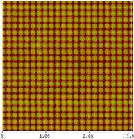
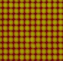
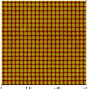
| SEM Image | Tapping Mode 3µm AFM scan | Contact Mode 5µm AFM scan | ||||
|
The above image (inset) was captured with a magnification setting of 100 kX and accelerating voltage 10 kV. Outside Image 20 kV. At 5 kX, the individual bumps were still well-resolved. Large fields of view show how few defects are present. The most common defects are single missing bumps or a single extra bump inserted between lattice positions. Two vacancies are present in the image shown here. |
 |
 During scanning in contact mode using a 0.5 N/m SiN cantilever, we did not notice any surface or tip wear affecting the image. |
||||
 Model 2DUTC Sample Certificate
Click images for dimensions