Description
2D Holographic Array Standards
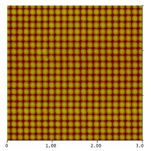
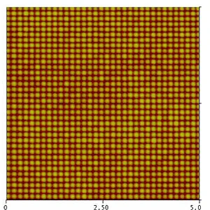
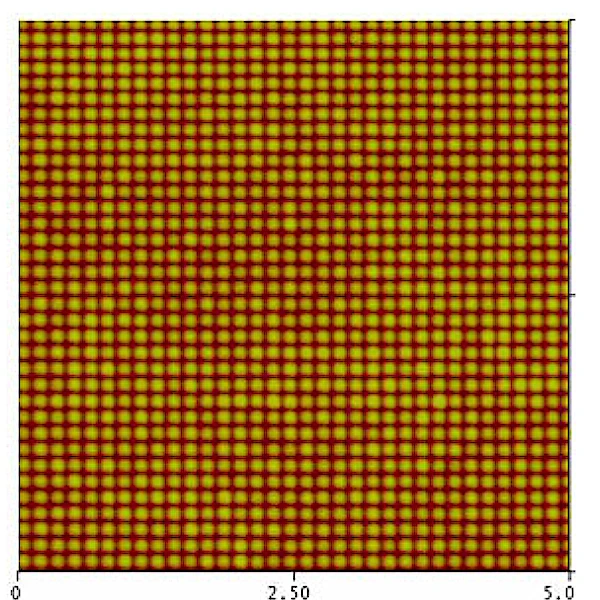
| Period: | 144nm pitch, two-dimensional array. Accurate to 1nm. Refer to calibration certificate for actual pitch.Surface:Aluminum bumps on Silicon, 4x3mm die. Bump height (about 90nm) and width (about 75nm) are not calibrated. |
| Usability: | The calibrated pattern covers the entire chip. There is sufficient usable area to make tens of thousands of measurements without reusing any areas altered or contaminated by previous scans. |
| AFM: | Use in contact, intermittent contact (TappingMode ) and other modes with image sizes from 250nm to 10 m. Available unmounted or mounted on 12mm steel disks. |
| SEM: | This specimen works well at all accelerating voltages. Normally supplied unmounted. Can be mounted on a stub of your choice of SEM Mount |
| Model 2D: | This Calibration Reference specimen comes with a non-traceable, manufacturer s certificate. This states the average period, based on batch measurements. |
| Model 2DUTC: | This Traceable, Certified Standard is a select grade. Each standard is individually measured in comparison with a similar specimen calibrated at PTB. (PTB, Physikalisch-Technischen Bundesanstalt, is the German counterpart of NIST.) The uncertainty of single pitch values is typically 1.4nm (95% confidence interval). Multi-pitch measurements provide the usual square-root of N improvement in precision. |