Description
2D Holographic Array Standards
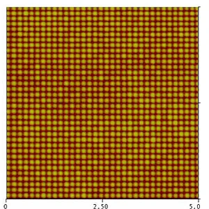
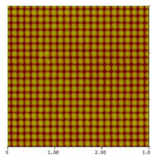
300nm Pitch High Resolution 2D Calibration Standard for AFM, STEM, SEM, Auger and FIB.
| Period: | 300nm pitch nominal, two dimensional array accurate to 1nm. Calibration certificate will give the actual pitch of the standard. |
| Surface Structure: | Aluminum bumps on Silicon, 4x3mm die: Bump height (about 50nm) and width (about 150nm) not calibrated. |
| Usability: | The calibrated pattern covers the entire chip. There is sufficient usable area to make thousands of measurements without reusing any areas contaminated or altered by previous scans. |
| AFM: | Use in contact, tapping and other modes with image sizes from 500nm to 20nm. Mounted on a 12mm steel AFM disk. |
| SEM: | Auger, FIB: Can be used for a wide range of accelerating voltage (1kV-20kV) and calibrates images from 5kX to 200kX. Can be supplied unmounted or mounted on an SEM stub of your choice, SEM Mount Selection A-R. |
| Certification: | Supplied with a non-traceable manufacturer’s certificate stating average pitch, based on batch measurements. |