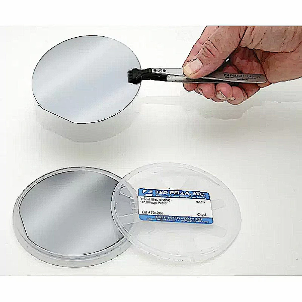
Description
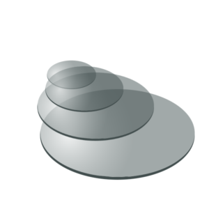
hese 1″, 2″, 3″, 4″ and 6″ (25.4, 50.8, 76.2, 100, 150mm) diameter silicon wafers can be used either as a substrate for thin film research or to make smaller substrates by dicing the wafer into pieces using Scribing and Cleaving Kits and hand tools. The wafer is shipped in a coin-style wafer carrier.
Properties:
- Orientation: <100> for 1″, 2″, 3″, 4″ and 6″ wafer <111> for 3″ P type
- Resistivity: 1-50 Ohm-cm
- Type P: (Boron) (1 primary flat)
- Type N: Phosphorous doped (1 primary flat)
- No SiO2 top coating
- Wafer thickness:
Ø1″ = 0.010 – 0.012″ (275 – 325µm)
Ø2″ = 0.010 – 0.012″(255 – 305µm)
Ø3″ = 0.013 – 0.017″ (330 – 420µm)
Ø4″ = 0.020 – 0.021″ (505 – 545µm)
Ø6″ = 0.023 – 0.027″ (585 – 695µm)
- Roughness: 2nm
- TTV: ≤5µm
- Bow/Warp: ≤30µm
- Wafer is polished on one side, etched on the other