Description
Pelcotec SFG12 Finder Grid Substrate
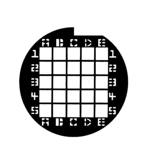
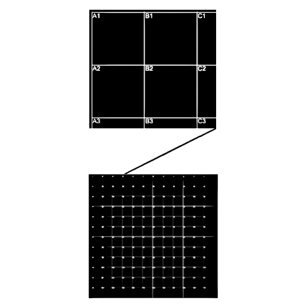
The innovative Pelcotec SFG12 finder grid substrate is a flat, conductive silicon substrate with a die size of 12.5 x 12.5mm.
It is covered with a 1 x 1mm raster giving a total of 12×12=144 fields.
Each field has a unique label using an alphanumeric pattern.
The lines and labels are precision laser etched in the silicon surface. It is the best combination of a flat specimen support and an SEM finder grid.
This unique and innovative product has some resemblance with an engraved SEM specimen mount, but it has a number of additional advantages:
- Flat – there are no height differences like with copper finder grids
- Fine pattern over a large area – better defined than engraved SEM mounts
- Low background signal – same as with Si chip substrates
- For EDX analysis only one element (Si) from the finder substrate
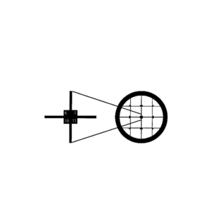
- Practical and easy to navigate – 1mm spacing with 144 fields
- Pattern is visible with naked eye, preparation microscope and SEM
- Gives an approximate size at (very) low magnification
- Can easily be mounted on SEM sample stubs – compatible with most popular sizes
- Can be used with SEM, FIB, XPS/ESCA, Auger and LM
Specifications of the silicon substrate used: prime virgin silicon wafer, P Boron doped, <100> orientation, resistivity of 0.5-35 ohm/cm, thickness 645 m 55 m.